- 您现在的位置:买卖IC网 > Sheet目录494 > NVTFS4824NTAG (ON Semiconductor)MOSFET N-CH 30V 18.2A 8WDFN
�� �
�
�NVTFS4824N�
�Power� MOSFET�
�30� V,� 4.7� m� W� ,� 46� A,� Single� N� ?� Channel�
�Features�
�?� Small� Footprint� (3.3� x� 3.3� mm)� for� Compact� Design�
�?� Low� R� DS(on)� to� Minimize� Conduction� Losses�
�?� Low� Capacitance� to� Minimize� Driver� Losses�
�?� NVTFS4824NWF� ?� Wettable� Flanks� Product�
�?� AEC� ?� Q101� Qualified� and� PPAP� Capable�
�?� These� Devices� are� Pb� ?� Free� and� are� RoHS� Compliant�
�V� (BR)DSS�
�30� V�
�http://onsemi.com�
�R� DS(on)� MAX�
�4.7� m� W� @� 10� V�
�7.5� m� W� @� 4.5� V�
�I� D� MAX�
�46� A�
�MAXIMUM� RATINGS� (T� J� =� 25� °� C� unless� otherwise� noted)�
�Parameter�
�Drain� ?� to� ?� Source� Voltage�
�Gate� ?� to� ?� Source� Voltage�
�Symbol�
�V� DSS�
�V� GS�
�Value�
�30�
�"� 20�
�Unit�
�V�
�V�
�N� ?� Channel�
�D� (5� ?� 8)�
�Continuous� Drain� Cur-�
�rent� R� Y� J� ?� mb� (Notes� 1,�
�2,� 3,� 4)�
�Power� Dissipation�
�R� Y� J� ?� mb� (Notes� 1,� 2,� 3)�
�Steady�
�State�
�T� mb� =� 25� °� C�
�T� mb� =� 100� °� C�
�T� mb� =� 25� °� C�
�T� mb� =� 100� °� C�
�I� D�
�P� D�
�46�
�33�
�21�
�11�
�A�
�W�
�G� (4)�
�S� (1,� 2,� 3)�
�T� A� =� 25� °� C�
�Continuous� Drain� Cur-�
�rent� R� q� JA� (Notes� 1,� 3,�
�&� 4)�
�Power� Dissipation�
�R� q� JA� (Notes� 1,� 3)�
�Pulsed� Drain� Current�
�T� A� =� 25� °� C�
�Steady� T� A� =� 100� °� C�
�State�
�T� A� =� 100� °� C�
�T� A� =� 25� °� C,� t� p� =� 10� m� s�
�I� D�
�P� D�
�I� DM�
�18.2�
�12.8�
�3.2�
�1.6�
�402�
�A�
�W�
�A�
�1�
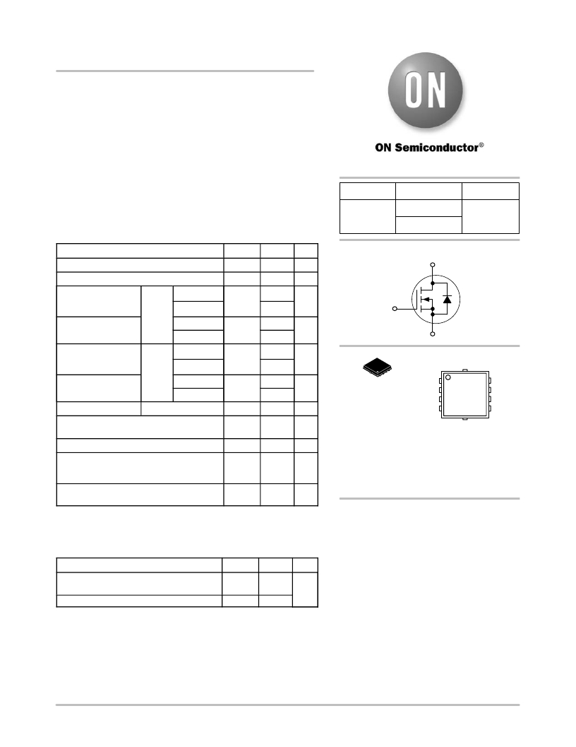
�WDFN8�
�(� m� 8FL)�
�CASE� 511AB�
�MARKING� DIAGRAM�
�1�
�S� D�
�S� XXXX� D�
�S� AYWW� G� D�
�G� G� D�
�Operating� Junction� and� Storage� Temperature�
�T� J� ,� T� stg�
�?� 55� to�
�175�
�°� C�
�XXXX�
�=� Specific� Device� Code�
�Source� Current� (Body� Diode)�
�Single� Pulse� Drain� ?� to� ?� Source� Avalanche�
�Energy� (T� J� =� 25� °� C,� V� DD� =� 50� V,� V� GS� =� 10� V,�
�I� L(pk)� =� 38� A,� L� =� 0.1� mH,� R� G� =� 25� W� )�
�Lead� Temperature� for� Soldering� Purposes�
�(1/8� ″� from� case� for� 10� s)�
�I� S�
�E� AS�
�T� L�
�21�
�72�
�260�
�A�
�mJ�
�°� C�
�A� =� Assembly� Location�
�Y� =� Year�
�WW� =� Work� Week�
�G� =� Pb� ?� Free� Package�
�(Note:� Microdot� may� be� in� either� location)�
�Stresses� exceeding� Maximum� Ratings� may� damage� the� device.� Maximum�
�Ratings� are� stress� ratings� only.� Functional� operation� above� the� Recommended�
�Operating� Conditions� is� not� implied.� Extended� exposure� to� stresses� above� the�
�Recommended� Operating� Conditions� may� affect� device� reliability.�
�THERMAL� RESISTANCE� MAXIMUM� RATINGS� (Note� 1)�
�ORDERING� INFORMATION�
�See� detailed� ordering,� marking� and� shipping� information� in� the�
�package� dimensions� section� on� page� 5� of� this� data� sheet.�
�Parameter�
�Junction� ?� to� ?� Mounting� Board� (top)� ?� Steady�
�State� (Notes� 2� and� 3)�
�Junction� ?� to� ?� Ambient� ?� Steady� State� (Note� 3)�
�Symbol�
�R� Y� J� ?� mb�
�R� q� JA�
�Value�
�7.2�
�47�
�Unit�
�°� C/W�
�1.� The� entire� application� environment� impacts� the� thermal� resistance� values� shown,�
�they� are� not� constants� and� are� only� valid� for� the� particular� conditions� noted.�
�2.� Psi� (� Y� )� is� used� as� required� per� JESD51� ?� 12� for� packages� in� which�
�substantially� less� than� 100%� of� the� heat� flows� to� single� case� surface.�
�3.� Surface� ?� mounted� on� FR4� board� using� a� 650� mm� 2� ,� 2� oz.� Cu� pad.�
�4.� Maximum� current� for� pulses� as� long� as� 1� second� is� higher� but� is� dependent�
�on� pulse� duration� and� duty� cycle.�
�?� Semiconductor� Components� Industries,� LLC,� 2013�
�May,� 2013� ?� Rev.� 2�
�1�
�Publication� Order� Number:�
�NVTFS4824N/D�
�发布紧急采购,3分钟左右您将得到回复。
相关PDF资料
NVTFS5116PLTWG
MOSFET P-CH 60V 14A 8WDFN
NVTFS5811NLTAG
MOSFET N-CH 40V 40A 8WDFN
NVTFS5820NLTAG
MOSFET N-CH 60V 37A 8WDFN
NVTFS5826NLTAG
MOSFET N-CH 60V 20A 8WDFN
NX201103
SYNJET ZFLOW 87 LEVEL SELECT 12V
NX300106
HEATSINK 43W TWIST GE INFUSION
NX300119
HEATSINK 70W SPOT CONFIG
NX300131
HEATSINK 58W TWIST MODULE COOLER
相关代理商/技术参数
NVTFS4824NTWG
功能描述:MOSFET N-CH 30V 18.2A 8WDFN RoHS:是 类别:分离式半导体产品 >> FET - 单 系列:- 标准包装:1,000 系列:MESH OVERLAY™ FET 型:MOSFET N 通道,金属氧化物 FET 特点:逻辑电平门 漏极至源极电压(Vdss):200V 电流 - 连续漏极(Id) @ 25° C:18A 开态Rds(最大)@ Id, Vgs @ 25° C:180 毫欧 @ 9A,10V Id 时的 Vgs(th)(最大):4V @ 250µA 闸电荷(Qg) @ Vgs:72nC @ 10V 输入电容 (Ciss) @ Vds:1560pF @ 25V 功率 - 最大:40W 安装类型:通孔 封装/外壳:TO-220-3 整包 供应商设备封装:TO-220FP 包装:管件
NVTFS4824NWFTAG
制造商:ONSEMI 制造商全称:ON Semiconductor 功能描述:30 V, 4.7 m, 46 A, Single Na??Channel
NVTFS4824NWFTWG
制造商:ONSEMI 制造商全称:ON Semiconductor 功能描述:30 V, 4.7 m, 46 A, Single Na??Channel
NVTFS4C10NTAG
制造商:ON Semiconductor 功能描述:NFET U8FL 30V 44A 7.4MOHM - Tape and Reel 制造商:ON Semiconductor 功能描述:NFET U8FL 30V 44A 7.4MOHM - Cut TR (SOS) 制造商:ON Semiconductor 功能描述:REEL / NFET U8FL 30V 44A 7.4MOHM
NVTFS5116PL
制造商:ONSEMI 制造商全称:ON Semiconductor 功能描述:Power MOSFET ?60 V, ?14 A, 52 m, Single P?Channel
NVTFS5116PLTAG
功能描述:MOSFET Single P-Channel 60V,14A,52mohm
RoHS:否 制造商:STMicroelectronics 晶体管极性:N-Channel 汲极/源极击穿电压:650 V 闸/源击穿电压:25 V 漏极连续电流:130 A 电阻汲极/源极 RDS(导通):0.014 Ohms 配置:Single 最大工作温度: 安装风格:Through Hole 封装 / 箱体:Max247 封装:Tube
NVTFS5116PLTWG
功能描述:MOSFET Single P-Channel 60V,14A,52mohm RoHS:否 制造商:STMicroelectronics 晶体管极性:N-Channel 汲极/源极击穿电压:650 V 闸/源击穿电压:25 V 漏极连续电流:130 A 电阻汲极/源极 RDS(导通):0.014 Ohms 配置:Single 最大工作温度: 安装风格:Through Hole 封装 / 箱体:Max247 封装:Tube
NVTFS5116PLWFTAG
制造商:ON Semiconductor 功能描述:PFET U8FL 60V 14A 52MOHM - Tape and Reel 制造商:ON Semiconductor 功能描述:Pwr MOSFET 60V 14A 52mOhm SGL P-CH 制造商:ON Semiconductor 功能描述:REEL - PFET U8FL 60V 14A 52MOHM